# HDMI
## Overview: You should learn VGA first!
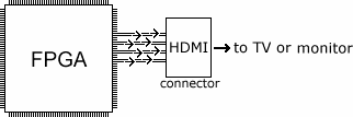
It's a common pattern to use a rgb-to-dvi ip core to recieve VGA signals and transform them to HDMI signals. So you don't need too much knowledge about HDMI. Remember our design pattern, which is shown below. Our rgb-to-dvi instance just lies in "Video Out".
I don't know the details about HDMI, I just list the key points.
## Key points
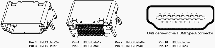
### Connector
A standard HDMI connector has 19 pins. Out of the 19 pins, 8 are of particular interest as they form 4 TMDS differential pairs to transport the actual high-speed video info.
* TMDS clock+ and clock-
* TMDS data0+ and data0-
* TMDS data1+ and data1-
* TMDS data2+ and data2-
{% hint style="info" %}
HDMI output enable is occasionally necessary, but most of the time it is not.
**Does HDMI needs synchronization signals? If answer is yes, where? If answer is no, why? (answered in later sections)**
{% endhint %}
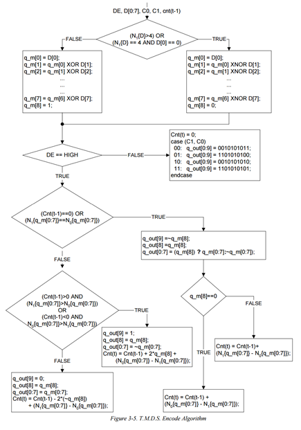
### TMDS
Video data travels on the **Transition Minimised Differential Signalling** (TMDS) physical layer in HDMI, same as DVI. TMDS signalling standard encodes 8 bits of each colour (RGB) into 10 bits. The information is then transmitted at 10x the speed of the pixel clock. This format is called `8b/10b`.
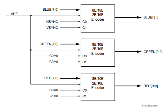
### Control data
`C0` and `C1` are control bits. We map **HSYNC** and **VSYNC** signals to the `C0` and `C1` ports of blue encoder. We set other control bits in green and red encoder 0.
{% hint style="info" %}
Why we only map the control signals to blue encoder?
{% endhint %}
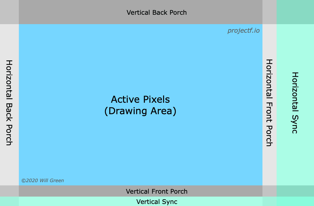
### Video timings
Similar to VGA.
## Source code
### TMDS encoder
The code comes from [fpga4fun](https://www.fpga4fun.com/HDMI.html). Thanks to the work of [Jean P. Nicolle](https://www.fpga4fun.com/SiteInformation.html).
```verilog
module TMDS_encoder (
input clk,
input [7:0] VD, // video data (red, green or blue)
input [1:0] CD, // control data
input VDE, // video data enable, to choose between CD (when VDE=0) and VD (when VDE=1)
output reg [9:0] TMDS = 0
);
wire [3:0] Nb1s = VD[0] + VD[1] + VD[2] + VD[3] + VD[4] + VD[5] + VD[6] + VD[7];
wire XNOR = (Nb1s>4'd4) || (Nb1s==4'd4 && VD[0]==1'b0);
wire [8:0] q_m = {~XNOR, q_m[6:0] ^ VD[7:1] ^ {7{XNOR}}, VD[0]};
reg [3:0] balance_acc = 0;
wire [3:0] balance = q_m[0] + q_m[1] + q_m[2] + q_m[3] + q_m[4] + q_m[5] + q_m[6] + q_m[7] - 4'd4;
wire balance_sign_eq = (balance[3] == balance_acc[3]);
wire invert_q_m = (balance==0 || balance_acc==0) ? ~q_m[8] : balance_sign_eq;
wire [3:0] balance_acc_inc = balance - ({q_m[8] ^ ~balance_sign_eq} & ~(balance==0 || balance_acc==0));
wire [3:0] balance_acc_new = invert_q_m ? balance_acc-balance_acc_inc : balance_acc+balance_acc_inc;
wire [9:0] TMDS_data = {invert_q_m, q_m[8], q_m[7:0] ^ {8{invert_q_m}}};
wire [9:0] TMDS_code = CD[1] ? (CD[0] ? 10'b1010101011 : 10'b0101010100) : (CD[0] ? 10'b0010101011 : 10'b1101010100);
always @(posedge clk) TMDS <= VDE ? TMDS_data : TMDS_code;
always @(posedge clk) balance_acc <= VDE ? balance_acc_new : 4'h0;
endmodule
```
{% hint style="info" %}
It's will take time to understand what's going on inside the module, but don't worry because we have a formidable weapon: **abstraction**.
{% endhint %}
### Simple rgb2dvi converter
```verilog
module simple_rgb2dvi(
// input signals
input clk_pix,
input clk_TMDS,
input hsync,
input vsync,
input de, // data enable
input [23:0] video_data, // video data {r, g, b}
// output signals
output TMDSp_clk,
output TMDSn_clk,
output [2:0] TMDSn_data,
output [2:0] TMDSp_data
);
//////////////////////////////////////////////////////////////////////////////////
reg [7:0] red, green, blue;
wire [9:0] TMDS_red, TMDS_green, TMDS_blue;
assign {red, green, blue} = video_data;
TMDS_encoder encode_R(.clk(clk_pix), .VD(red ), .CD(2'b00) , .VDE(de), .TMDS(TMDS_red));
TMDS_encoder encode_G(.clk(clk_pix), .VD(green), .CD(2'b00) , .VDE(de), .TMDS(TMDS_green));
TMDS_encoder encode_B(.clk(clk_pix), .VD(blue ), .CD({vsync,hsync}), .VDE(de), .TMDS(TMDS_blue));
//////////////////////////////////////////////////////////////////////////////////
reg [3:0] TMDS_mod10 = 0; // modulus 10 counter
reg [9:0] TMDS_shift_red = 0, TMDS_shift_green = 0, TMDS_shift_blue = 0;
reg TMDS_shift_load=0;
always @(posedge clk_TMDS) TMDS_shift_load <= (TMDS_mod10 == 4'd9);
always @(posedge clk_TMDS) begin
TMDS_shift_red <= TMDS_shift_load ? TMDS_red : TMDS_shift_red [9:1];
TMDS_shift_green <= TMDS_shift_load ? TMDS_green : TMDS_shift_green[9:1];
TMDS_shift_blue <= TMDS_shift_load ? TMDS_blue : TMDS_shift_blue [9:1];
TMDS_mod10 <= (TMDS_mod10 == 4'd9) ? 4'd0 : TMDS_mod10 + 4'd1;
end
assign TMDSp_data[2] = TMDS_shift_red;
assign TMDSp_data[1] = TMDS_shift_green;
assign TMDSp_data[0] = TMDS_shift_blue;
assign TMDSn_data[2] = ~TMDS_shift_red;
assign TMDSn_data[1] = ~TMDS_shift_green;
assign TMDSn_data[0] = ~TMDS_shift_blue;
assign TMDSp_clk = clk_pix;
assign TMDSn_clk = ~clk_pix;
endmodule
```
{% hint style="info" %}
We often use third-party rgb2dvi IP cores.
{% endhint %}
### Put it all together
#### generate clock\_480p using IP cores
{% hint style="info" %}
Don't leave it at the default settings. That will not work!
{% endhint %}
#### signal\_480p.sv
```verilog
module signal_480p (
input wire logic clk_pix, // pixel clock
input wire logic rst_pix, // reset in pixel clock domain
output logic [9:0] sx, // horizontal screen position
output logic [9:0] sy, // vertical screen position
output logic hsync, // horizontal sync
output logic vsync, // vertical sync
output logic de // data enable (low in blanking interval)
);
// horizontal timings
parameter HA_END = 639; // end of active pixels
parameter HS_STA = HA_END + 16; // sync starts after front porch
parameter HS_END = HS_STA + 96; // sync ends
parameter LINE = 799; // last pixel on line (after back porch)
// vertical timings
parameter VA_END = 479; // end of active pixels
parameter VS_STA = VA_END + 10; // sync starts after front porch
parameter VS_END = VS_STA + 2; // sync ends
parameter SCREEN = 524; // last line on screen (after back porch)
always_comb begin
hsync = ~(sx >= HS_STA && sx < HS_END); // invert: negative polarity
vsync = ~(sy >= VS_STA && sy < VS_END); // invert: negative polarity
de = (sx <= HA_END && sy <= VA_END);
end
// calculate horizontal and vertical screen position
always_ff @(posedge clk_pix) begin
if (sx == LINE) begin // last pixel on line?
sx <= 0;
sy <= (sy == SCREEN) ? 0 : sy + 1; // last line on screen?
end else begin
sx <= sx + 1;
end
if (rst_pix) begin
sx <= 0;
sy <= 0;
end
end
endmodule
```
#### painter\_480p.sv
```verilog
module painter_480p (
input wire logic clk_pix,
input wire logic [9:0] sx,
input wire logic [9:0] sy,
output logic [7:0] rgb_r,
output logic [7:0] rgb_g,
output logic [7:0] rgb_b
);
wire [7:0] W = {8{sx[7:0]==sy[7:0]}};
wire [7:0] A = {8{sx[7:5]==3'h2 && sy[7:5]==3'h2}};
always @(posedge clk_pix) rgb_r <= ({sx[5:0] & {6{sy[4:3]==~sx[4:3]}}, 2'b00} | W) & ~A;
always @(posedge clk_pix) rgb_g <= (sx[7:0] & {8{sy[6]}} | W) & ~A;
always @(posedge clk_pix) rgb_b <= sy[7:0] | W | A;
endmodule
```
#### top.sv
```verilog
module top (
input sys_clk,
output TMDSn_clk,
output TMDSp_clk,
output [2:0] TMDSn_data,
output [2:0] TMDSp_data
);
////////////////////// clock generator ////////////////////
wire clk_pix, clk_TMDS;
clock_480p clock_480p_m0 (
.clk_in1(sys_clk),
.clk_out1(clk_pix),
.clk_out2(clk_TMDS),
.reset(1'b0),
.locked()
);
////////////////////// signal generator ////////////////////
wire [9:0] sx, sy;
wire hsync, vsync, de;
signal_480p signal_480p_m0 (
.clk_pix,
.rst_pix(1'b0),
.sx,
.sy,
.hsync,
.vsync,
.de
);
////////////////////// drawing logic ////////////////////
reg [7:0] rgb_r, rgb_g, rgb_b;
painter_480p painter_480p_m0 (
.clk_pix,
.sx,
.sy,
.rgb_r,
.rgb_g,
.rgb_b
);
////////////////////// rgb2dvi converter ////////////////////
simple_rgb2dvi simple_rgb2dvi_m0 (
.clk_pix,
.clk_TMDS,
.hsync,
.vsync,
.de,
.video_data({rgb_r, rgb_g, rgb_b}),
// output signals
.TMDSp_clk,
.TMDSn_clk,
.TMDSn_data,
.TMDSp_data
);
endmodule
```
{% hint style="info" %}
Use PLL or MMCM ip cores to generate pixel clock and TMDS clock.
{% endhint %}
### Test
Our test board is ZYNQ7000 AX7020. The pins assignment file is given at [ZYNQ7000-AX7020.xdc](https://github.com/byrzhm/digital-design/blob/main/FPGA/hdmi_test/ZYNQ7000_AX7020.xdc).
```
set_property PACKAGE_PIN U18 [get_ports sys_clk]
set_property IOSTANDARD LVCMOS33 [get_ports sys_clk]
create_clock -period 20.000 -waveform {0.000 10.000} [get_ports sys_clk]
#set_property PACKAGE_PIN V16 [get_ports hdmi_oen]
#set_property IOSTANDARD LVCMOS33 [get_ports hdmi_oen]
set_property PACKAGE_PIN V20 [get_ports {TMDSp_data[0]}]
set_property IOSTANDARD LVCMOS33 [get_ports {TMDSp_data[0]}]
set_property PACKAGE_PIN W20 [get_ports {TMDSn_data[0]}]
set_property IOSTANDARD LVCMOS33 [get_ports {TMDSn_data[0]}]
set_property PACKAGE_PIN T20 [get_ports {TMDSp_data[1]}]
set_property IOSTANDARD LVCMOS33 [get_ports {TMDSp_data[1]}]
set_property PACKAGE_PIN U20 [get_ports {TMDSn_data[1]}]
set_property IOSTANDARD LVCMOS33 [get_ports {TMDSn_data[1]}]
set_property PACKAGE_PIN N20 [get_ports {TMDSp_data[2]}]
set_property IOSTANDARD LVCMOS33 [get_ports {TMDSp_data[2]}]
set_property PACKAGE_PIN P20 [get_ports {TMDSn_data[2]}]
set_property IOSTANDARD LVCMOS33 [get_ports {TMDSn_data[2]}]
set_property PACKAGE_PIN N18 [get_ports TMDSp_clk]
set_property IOSTANDARD LVCMOS33 [get_ports TMDSp_clk]
set_property PACKAGE_PIN P19 [get_ports TMDSn_clk]
set_property IOSTANDARD LVCMOS33 [get_ports TMDSn_clk]
```
Here is our screen output.
## References
{% embed url="" %}
{% embed url="" %}
{% embed url="" %}
{% embed url="" %}
{% embed url="" %}
---
# Agent Instructions: Querying This Documentation
If you need additional information that is not directly available in this page, you can query the documentation dynamically by asking a question.
Perform an HTTP GET request on the current page URL with the `ask` query parameter:
```
GET https://byrzhm.gitbook.io/build-a-risc-v-chip-from-scratch/interfaces/graphics/hdmi.md?ask=
```
The question should be specific, self-contained, and written in natural language.
The response will contain a direct answer to the question and relevant excerpts and sources from the documentation.
Use this mechanism when the answer is not explicitly present in the current page, you need clarification or additional context, or you want to retrieve related documentation sections.